Two Nanostructures Are Better Than One

Imagine using minuscule structures the size of molecules to harvest sunlight and convert it into electricity. Or employing the same structures to store hydrogen fuel so that it fits into a car’s gas tank. Or replacing today’s semiconductors with these structures, ushering in the next generation of small, powerful electronics.
These technologies don’t exist yet, but the work of a researcher at the University of Wisconsin-Milwaukee (UWM) is bringing them closer to reality with hybrid materials made with carbon nanotubes (CNTs).
Junhong Chen, assistant professor of mechanical engineering, is pioneering better methods of making CNTs more predictable.
CNTs are invisibly thin sheets of graphite that are rolled into a cylindrical shape. Chen’s laboratory focuses on new uses for CNTs combined with nanoparticles, bits of matter that are nanoscale in all three dimensions.
“These interesting multi-component structures will open up new opportunities in several interdisciplinary fields,” Chen says, “including medical diagnostics, green energy technology, and sensors for everything from food flavor to invisible toxic gas.”
Big and small worlds collide
CNTs are the potential superstar structures of molecular engineering because of their remarkable electronic and mechanical properties. Already they are used in making flat panel display screens and sensing devices that can detect substances in very low concentrations.
They conduct electricity like either copper or silicon, are stronger than steel, pliable like polymers (kinds of plastics) and can be made from a range of raw materials.
The challenge is to coax them to behave in predictable ways.
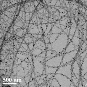
With the help of graduate student Ganhua Lu, Chen has devised a method for creating hybrid structures by coating CNTs with aerosol nanoparticles. His lab also has produced a low-cost way to make “custom” nanoparticles that gives them full control over the structure’s final properties.
Manipulating CNTs and nanoparticles is tricky business because so many conditions affect their behavior. Just below nanoscale, at the level of individual atoms, matter acts quite differently than it does lumped together in bulk.
Already they have devised a gas sensor using only nanoparticles of tin oxide.
Their process for producing hybrid structures is far superior to the method currently available, and their work advances understanding of how materials in the quantum world interact with those in the “seen” world.
Surface science cluster at UWM
“My goal is to make something real, that people can see and use and that has tangible results,” says Chen, who came to UWM in 2003 after a year as a post-doctoral scholar at the California Institute of Technology.
With two patents pending and funding from sources such as the National Science Foundation and the Xerox Corporation, he is well on his way.
Chen is one of a cluster of UWM scientists – in engineering, chemistry and physics – who conduct research into nano- and surface science. In fact, UWM’s Laboratory for Surface Studies, a University of Wisconsin System Center of Excellence, brings together the work of 13 faculty who explore the structure and properties of solid surfaces and the interaction of surfaces with atoms and molecules.
The lab’s research encompasses topics such as thin films and laminates, spintronics, molecular wires, optical fiber sensing, and properties such as catalysis, corrosion and friction.
New materials, cool features
When it comes to size, there’s tiny and then there’s tiny all over. Nanostructures can be at nanoscale in either one, two or three dimensions, or any combination. The structure’s properties are determined by the number of dimensions at nanoscale, its shape, and the material it’s made of.
CNTs, for example, can behave like an electrical conductor or a semiconductor, depending on the diameter and the twist of the tube. Nanoparticles have their own unique characteristics. Once attached to CNTs, they can transfer their abilities to the tube.
Nanoparticles could potentially give an insulator like silicon the ability to conduct electricity.
A happy union of the two structures offers a chance to brainstorm new applications, says Chen. For example, the hybrid can be altered to absorb and emit various wavelengths of light, giving it optical properties.
“You get an opportunity to make a material that could potentially display not only the properties of the CNT and the nanoparticles, but also some additional properties because of the interaction between the two.
“So one plus one may be greater than two,” he says. “That’s the whole idea.”
Molecular building with control
Before Chen’s technique for fusing the two nanostructures, the process took hours.
CNTs are produced in a gas phase from carbon precursors, but nanoparticles are made in a solution, he says. “You had to combine the dry with the wet before you can make something out of it,” he says. “It’s not very compatible.”
Also the surface of each structure had to be modified, and the chemistry would be different for each new material involved.
“What you would get at the end could be very different from what you were trying to get,” he says.
So Chen and his lab developed a way to make nanoparticles in the gas (dry) phase. Then they applied an electrostatic force to attract any kind of nanoparticle to the CNT. The one-step process takes only minutes.
“It works like an indoor air cleaner, using the electric field to capture dust particles,” he says.
Another advantage of the process is Chen can control the size of the nanoparticle that is fastened to the tube, and that determines the final properties of the hybrid structure. The higher the electric field, the larger the particles it will attract.
Chen believes the research has huge potential.
“Many of our projects lie at the intersection of fundamental science and industrial applications with ample opportunities for new discoveries.”
Source: University of Wisconsin - Milwaukee


