Novel gate dielectric materials: perfection is not enough

For the first time theoretical modeling has provided a glimpse into how promising dielectric materials are able to trap charges, something which may affect the performance of advanced electronic devices. This is revealed in a paper published on the 12th October in ������Ƶical Review Letters by researchers at the London Centre for ������Ƶ and SEMATECH, a company in Austin, Texas.
Through the constant quest for miniaturization, transistors and all their components continue to decrease in size. A similar reduction has resulted in the thickness of a component material known as the gate dielectric – typically a thin layer of silicon dioxide, which has now been in use for decades.
Unfortunately, as the thickness of the gate dielectric decreases, silicon dioxide begins to leak current, leading to unwieldy power consumption and reduced reliability. Scientists hope that this material can be replaced with others, known as high-dielectric constant (or high-k) dielectrics, which mitigate the leakage effects at these tiny scales.
Metal oxides with high-k have attracted tremendous interest due to their application as novel materials in the latest generation of devices. The impetus for their practical introduction would be further helped if their ability to capture and trap charges and subsequent impact on instability of device performance was better understood.
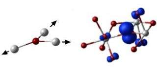
It has long been believed that these charge-trapping properties originate from structural imperfections in materials themselves. However, as is theoretically demonstrated in this publication, even if the structure of the high k dielectric material is perfect, the charges (either electrons or the absence of electrons – known as holes) may experience ‘self trapping’.
They do so by forming polarons – a polarizing interaction of an electron or hole with the perfect surrounding lattice. Professor Alexander Shluger of the London Centre for ������Ƶ and the Department of ������Ƶics & Astronomy at UCL says: “This creates an energy well which traps the charge, just like a deformation of a thin rubber film traps a billiard ball.”
The resulting prediction is that at low temperatures electrons and holes in these materials can move by hopping between trapping sites rather than propagating more conventionally as a wave. This can have important practical implications for the materials’ electrical properties. In summary, this new understanding of the polaron formation properties of the transition metal oxides may open the way to suppressing undesirable characteristics in these materials.
Source: University College London


