New method for making graphene turns defects into improvements

Alexander Pol
deputy editor

Recent research has found a new way to make graphene that adds structural defects to improve the performance of the material that could have benefits across a range of applications—from sensors and batteries, to electronics.
Scientists from the University of Nottingham's School of Chemistry, University of Warwick and Diamond Light Source developed a single-step process to grow graphene-like films using a molecule, Azupyrene, whose shape mimics that of the desired defect. The research has been today in Chemical Science.
David Duncan, Associate Professor at the University of Nottingham and one of the study's lead authors, explains, "Our study explores a new way to make graphene, this super-thin, super-strong material is made of carbon atoms, and while perfect graphene is remarkable, it is sometimes too perfect. It interacts weakly with other materials and lacks crucial electronic properties required in the semiconductor industry."
"Usually defects in material are seen as problems or mistakes that reduce performance, we have used them intentionally to add functionality. We found the defects can make the graphene more 'sticky' to other materials, making it more useful as a catalyst, as well as improving its capability of detecting different gases for use in sensors. The defects can also alter the electronic and magnetic properties of the graphene, for potential applications in the semiconductor industry."
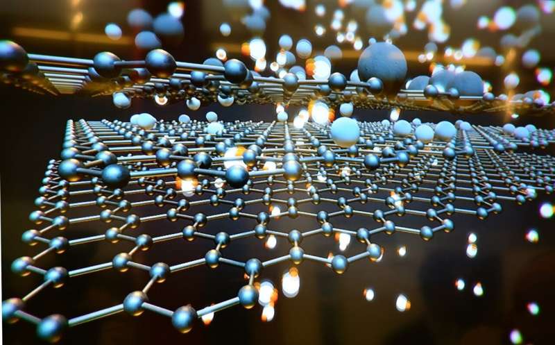
Graphene is made up of a flat tiling of six carbon atoms in a ring. The desired defect has neighboring rings consisting of 5 and 7 carbon atoms. Azupyrene has a shape (or topology) that naturally includes the same kind of irregular rings to be introduced into graphene. Azupyrene was used to grow graphene to create films with a high rate of this specific type of defect and, by changing the temperature during growth, the amount of defects in the final material could be controlled.
Researchers at the Graphene Institute in Manchester also successfully demonstrated that the graphene could be transferred onto different surfaces retaining the defects, a key technological achievement towards applying these films to actual devices.
This work used a wide range of advanced tools, bringing together a collaboration across the UK, Germany and Sweden using advanced microscopy and spectroscopy at Diamond Light Source in Oxfordshire and MAX IV in Sweden, as well as the UK national supercomputer ARCHER2, allowing the researchers to study the atomic structure of the defective graphene, demonstrating that the defects were present, and how the defects affected the chemical and electronic properties of the defective graphene.
Professor Reinhard Maurer, Department of Chemistry, University of Warwick, says, "By carefully choosing the starting molecule and the growth conditions, we've shown it's possible to grow graphene in which imperfections can be introduced in a more controlled way. We characterize the signatures of these imperfects by bringing together atomic-scale imaging, spectroscopy, and computational simulation."
"This study is a testament to what can be achieved through international collaboration and the integration of diverse scientific expertise," said Dr. Tien-Lin Lee from Diamond Light Source. "By combining advanced microscopy, spectroscopy, and computational modeling across institutions in the UK, Germany, and Sweden, we were able to uncover the atomic-scale mechanisms behind defect formation in graphene, something no single technique or team could have achieved alone."
More information: Benedikt P Klein et al, One-step synthesis of graphene containing topological defects, Chemical Science (2025).
Journal information: Chemical Science
Provided by University of Nottingham


