Collaboration yields 'the right glasses' for observing mystery behavior in electrons

In collaboration with the Center for Integrated Nanotechnologies at Los Alamos, an international team of researchers has, for the first time, viewed on a nanoscale the formation of mysterious metallic puddles that facilitate the transition of an electrically insulating material into an electrically conducting one.
The research may lead to a better understanding of superconductors—materials that conduct electricity without energy loss—or development of better materials for powering high-speed electronics.
In a paper published today in Science, Los Alamos researcher Alexander Balatsky joins researchers in describing a novel approach to viewing Mott transition in vanadium dioxide. Balatsky’s co-authors include: Mumtaz Qazilbash, Greg Andreev, Brian Maple and Dimitri Basov of the University of California-San Diego; Markus Brehm and Fritz Keilmann of the Max Planck Institute for Biochemistry and Center for NanoScience in Munich, Germany; and Byung-Gyu Chae, Hyun-Tak Kim and Sun Jin Yun of IT Convergence and Components Lab, Electronics and Telecommunication Research Institute in Korea.
Materials such as copper metal contain electrons that are mobile enough to conduct an electrical current. In conducting materials such as copper or aluminum, electrons do not hinder one another and are free to move about the lattice structure of the material. In more-complex crystal oxides, such as vanadium dioxide, electrons can become influenced by nearby positively or negatively charged particles, and their movement can become hindered. These materials are known by physicists as “correlated materials.”
Correlated materials include superconductors or semiconductors—crystals peppered or “doped” with atoms that may donate mobile electrons to the solid. Correlated materials can exhibit extraordinary changes in their physical properties, such as transforming from an insulating material to a conducting material, when subjected to relatively small changes in pressure or temperature.
Vanadium dioxide begins to transform itself from an insulator to a conductor when heated above 341 degrees Kelvin (about 154 degrees Fahrenheit or 68 degrees Celsius).
For decades scientists have puzzled over how this transformation to a fully metallic state—known as “Mott” metal-insulator transition—occurs. Balatsky, a Los Alamos condensed-matter theorist, believed, like many other scientists, that the transition begins when metallic puddles begin forming at sites of impurities or imperfections within the lattice. The puddles grow until they touch, and at that point the material becomes conductive, or superconductive.
“We had evidence to believe that metallic puddles were forming in an inhomogenous manner within the material at the transition phase, but we had no way of proving it,” said Balatsky. “If you had the right glasses that could see something extremely small, you could see this process occurring.”
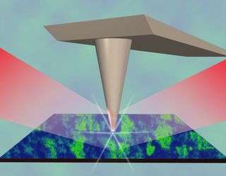
The ‘right glasses’ came in the form of a microscopic viewing technique known as near-field scanning optical microscopy, which has been used to inspect viruses and nano-transistors. The microscope sees infrared light reflecting off of a surface only 20-billionths of a meter (or 20 nanometers) wide. A single virus is less than 20 nanometers wide, while a typical human hair is about 100,000 nanometers wide.
Using this nanoscale viewer, the UCSD-LANL-Max Planck-ETRI team was able to watch metallic puddles form within vanadium oxide at the exact temperature where the Mott transition was expected to occur. These “infrared nanoscope” images have revealed for the first time a new type of metal “phase” existing only during the transition of the material from its insulating state to its conducting state.
The new findings will help researchers worldwide better describe and understand underlying physical laws of how charges propagate through correlated materials.
The research could help materials scientist understand how to precisely dope a material with specific atoms in order to optimize conducting or superconducting behavior or, conversely, to create materials impervious to electrical conductivity or magnetic influences.
“What is extremely exciting about this research is that four different laboratories with complementary disciplines cooperated to use this infrared nanoscope in its first successful application for solving a solid-state physics puzzle,” Keilmann said.
Source: Los Alamos National Laboratory


