December 22, 2020 feature
Two dimensional heterostructures composed of layers with slightly different lattice vectors

Thamarasee Jeewandara
contributing writer

New periodic structures known as moiré lattices can be observed in two-dimensional (2-D) heterostructures containing layers with slightly different lattice vectors, which can in turn support new topological phenomena. It is therefore important to obtain high-resolution imaging of these moiré lattices and superstructures to understand the emerging physics. In a new report now published in Science Advances, Kyunghoon Lee and a team of scientists report the imaging process to view moiré lattices and superstructures in graphene-based samples under ambient conditions using with ultrahigh-resolution implementation. While the probe tip of the device maintained a gross radius of 100 nm, the research team achieved a spatial resolution better than 5 nm. This setup allowed direct visualization of moiré lattices and the composite super-moiré. The researchers also showed the artificial synthesis of new superstructures arising from the interplay between diverse layers.
Topological physics and new quantum phenomena with moiré lattices
Two-dimensional heterostructures composed of atomically thin layers with slightly different lattice vectors can form moiré lattices with a large periodicity due to a large lattice mismatch or a small-angle twist in the structure. Such architectures generate a new length and energy scales in stacked 2-D materials to provide an exciting new platform to engineer in van der Waals heterostructures. Superstructures of moiré lattices can be formed when similar lattice structures are stacked together to offer extra flexibility to design new quantum phenomena. It is important to characterize the moiré lattice and superstructures in a device configuration to understand and control the rich moiré physics in 2-D heterostructures.
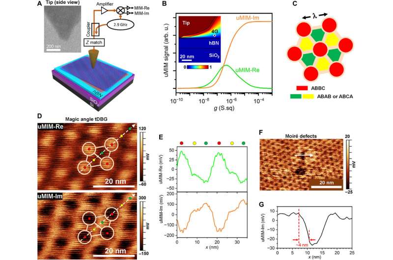
Traditionally this can be accomplished with (TEM), (AFM) and (STM) techniques. But most methods require specialized sample preparation protocols that are largely unsuited to observe functional devices. Scanning microwave impedance microscopy (sMIM) is an alternative and attractive moiré imaging tool compared to existing methods, which combines the benefit of spatial resolution with high sensitivity of local electrical properties of the device. Lee et al. therefore demonstrated an ultra-high-resolution implementation of sMIM, which they also named uMIM to perform nanoscale imaging of moiré lattices and superstructures of various graphene-based devices under ambient conditions.

Ultra-high-resolution scanning microwave impedance microscopy
Using the imaging probe, the team revealed several moiré superstructures including a supermodulation of the moiré lattice and a new Kagome-like moiré structure arising from the interplay between closely aligned twisted graphene and . Such moiré superstructures can offer new avenues to engineer quantum phenomena in van der Waals heterostructures. During the experiments, the team used the microscope to probe the local complex . The observed tip-sample admittance depended on the local sample conductivity and the team calculated the real and imaginary uMIM signals (as uMIM-Re and uMIM-Im respectively). The imaginary signal was informative to rapidly assess the local conductivity since it increased monotonically with the sheet conductance of the sample. The new analytical imaging method provided a microwave version of the method. Although unlike the near-field microscope, the researchers performed the experiments at contact mode where the electromagnetic coupling between the tip and sample was highly localized at the apex of the tip.

Proof-of-concept with graphene-based systems
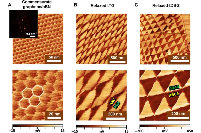
The team showed the capability of the imaging technique by viewing the moiré superlattice in (tDBG). They resolved three different domains in the tDBG moiré lattice using distinct signals to show the usefulness of the technique to identify fine structures of moiré lattices in 2-D heterostructures based on local conductivity. To demonstrate the spatial resolution capability of the method, Lee et al. imaged moiré defects along the moiré lattice, and resolved the defects with sub-5-nm resolution. This method outperformed other optical near-field microscopes.
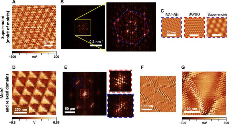
The scientists then showed the universal applicability of the method to resolve moiré structures in a variety of graphene-based systems. For example, the technique facilitated moiré observations in epitaxially grown monolayer graphene/hBN (hexagonal boron nitride) samples, synthesized using . The method also resolved the triangular domains in twisted trilayer graphene (tTG) and twisted double bilayer graphene (tDBG). Apart from conventional moiré lattices, the ultra-high sensitivity microscopic method also allowed imaging of moiré superstructures from three underlying lattices with different lattice vectors, such as twisted double bilayer graphene on hexagonal boron nitride (BG/BG/hBN). While such heterostructures have been previously imaged with conventional techniques, they remain to be . The topographic images showed modifications of the moiré structure, which may lead to a modified electronic spectrum that eventually may need to be included in theoretical calculations of the material's electronic structure.
Investigating other moiré superstructures
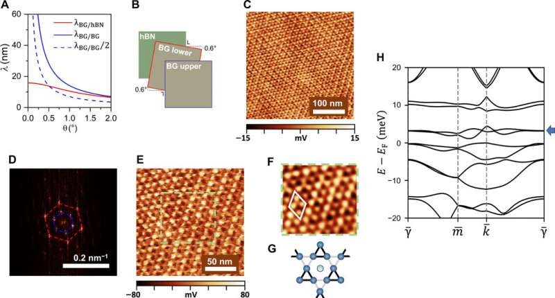
Lee et al. then used the method to investigate other moiré superstructures with desirable physical properties. For instance, the has attracted due to the presence of flat bands and exotic quantum and magnetic phases. However, Kagome lattice crystals are relatively rare in nature, while they can be simulated via an optical superlattice in . The team therefore developed a solid-state Kagome-like moiré superlattice in BG/BG/hBN (twisted double bilayer graphene on hexagonal boron nitride) systems and visualized a special moiré composite via the imaging technique. The scientists examined the resulting structure in detail and compared it with the expected structure of an ideal Kagome lattice.

Outlook
In this way, Kyunghoon Lee and colleagues extensively demonstrated the use of an ultrahigh resolution scanning microwave impedance microscope (sMIM) as a simple, high-throughput and noninvasive method to characterize moiré superlattices and superstructures including moiré defects. The team also tailored Kagome superlattices in multilayer stacks of graphene-based van der Waals heterostructures. The superior imaging technique will provide better understanding of the heterostructure design paths to investigate their correlation with quantum phenomena in advanced moiré superstructures.
Written for you by our author —this article is the result of careful human work. We rely on readers like you to keep independent science journalism alive. If this reporting matters to you, please consider a (especially monthly). You'll get an ad-free account as a thank-you.
More information: 1. Lee K et al. Ultrahigh-resolution scanning microwave impedance microscopy of moiré lattices and superstructures, Science Advances, 10.1126/sciadv.abd1919
2. Chen G. et al. Tunable correlated Chern insulator and ferromagnetism in a moiré superlattice, Nature,
3. Utama M. I. B. et al. Visualization of the flat electronic band in twisted bilayer graphene near the magic angle twist., Nature ������Ƶics,
Journal information: Nature ������Ƶics , Science Advances , Nature
© 2020 Science X Network


